Translucent Presents Novel Mirrored Si™ Process for Low-Cost LED Growth
Translucent GaN-on-Si wafer template with embedded DBR mirrors enables low-cost LED growth, the novel Mirrored Si™ process will be presented in a special session at the International Conference on Nitride Semiconductors in Glasgow, Scotland.
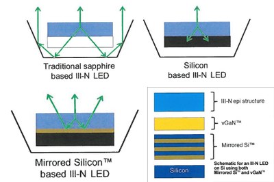
Translucent, Inc., a provider of rare-earth-oxide (REO) engineered silicon substrates for low-cost, high-performance epitaxy, announces that it has developed a proprietary GaN-on-Si wafer template with embedded DBR mirrors for application to low-cost LED growth.
This structure and the process used to grow it will be explained at the International Conference on Nitride Semiconductors (ICNS-9), Glasgow, Scotland, (July 15th, 2011) in a special post-deadline paper titled “Integrated High Reflectivity Silicon Substrates for GaN LEDs” (Session LN-2 at 8:30 AM GMT). View a copy of the presentation on the Translucent website.
Translucent will report technical details in the development of a 100-mm-diameter wafer that exhibits high reflectivity using a lattice-matched rare-earth-oxide material grown onto a silicon substrate. This structure is capped by a GaN layer that can support further nitride epitaxy for the growth of LED structures.
The lattice engineering offered by the rare earth oxide (REO) material system, which is grown epitaxially on silicon (111) substrates, can be utilized to mitigate strain arising during growth of GaN. REO materials further enable highly reflective mirrors embedded in engineered silicon substrates. The new technology is being offered to prospective customers who are ready to grow LEDs on large-diameter wafers.
Translucent’s silicon solution mitigates the need to remove the substrate and the use of handle wafers during subsequent processing. As the LED industry migrates to larger wafer sizes, a one-step epitaxial solution is expected to provide the best path to cost-effective scaling.
With Translucent’s new embedded silicon solution (Mirrored Si™), LEDs can now be grown directly on top of the GaN-on-Si template that includes an embedded DBR mirror, directly lattice matched to the silicon substrate. On top of this DBR mirror is a layer of proprietary patented Rare Earth Oxide (REO), which allows GaN to cap the template and does not require subsequent removal of the substrate.
Translucent’s paper describes how this device-ready GaN template can be supplied to LED manufacturers as-is for LED growth. Calculations are made that show that mirror reflectivity can exceed 98% at the LED-emitted wavelength range of 450 nm in ultra-thin layers of lattice-matched REO material.
The material was grown using molecular beam epitaxy (MBE) reactors at Translucent’s facilities. The exceptional quality of the growth achieved to date leads to extremely high quality crystalline interfaces which are scalable to large-diameter silicon wafers, thus indicating excellent commercial prospects for Translucent’s embedded mirror material.
Translucent is currently preparing to scale its embedded silicon mirror technology for commercial rollout with 150 mm and 200 mm wafers.
For additional information on Translucent's Technology please visit www.translucentinc.com/ or downlod the application note at http://www.translucentinc.com/documents/appnote_msi.pdf
About Translucent:
Translucent, Inc., a subsidiary of Australian listed company Silex Systems Limited. (SLX: ASX), is a materials-based company founded in 2001 that focuses on using rare-earth oxides to provide low-cost, silicon-based templates for epitaxial growth of semiconductors. With its emphasis on GaN- and Ge-compatible growth platforms, Translucent provides products for the solar, power FET, and solid-state lighting (LED) industries. Mirrored Si is a registered trademark of Translucent, Inc. More information is available at www.translucentinc.com and www.silex.com.au


