Photonics crystals improve LED efficiency
A 50% increase in efficiency is a significant stride toward being viable sources for solid-state lighting.
Light-emitting diodes (LEDs) based on indium gallium nitride (InGaN) will be used future high-efficiency lighting applications. Currently-available semiconductor-based white-light InGaN LEDs are more efficient than incandescent lightbulbs but still less efficient than fluorescent tubes. LEDs are currently limited by poor internal quantum and light-extraction efficiency, but photonic crystals offer a potential solution to both problems.
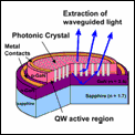
Our group, which has had solid-state-lighting research has been a major thrust since the late 1990s is now working to incorporate photonic crystals into LEDs. The internal quantum efficiency of InGaN LEDs can be enhanced via the Purcell effect, 1 in which the radiative recombination rate is increased (more photons are generated) by placing the emitters inside an optical cavity. Another way to improve output is to assist in the extraction of light from the high-index semiconductor chip. For typical InGaN LEDs, a large fraction of the energy is emitted into waveguided modes internal to the semiconductor rather than radiation modes. Light generated inside the semiconductor bounces around due to total internal reflection, and there is a high probability that the light will be absorbed before it can escape from the semiconductor. A photonic crystal 2 can improve light extraction by diffracting waveguided modes out of the semiconductor. Figure 1 shows a schematic diagram of a photonic crystal LED.
Figure 1. Incorporating a photonic crystal into an indium-gallium-nitride LED increases both the internal quantum efficiency and the amount of light extracted. The light is produced in the quantum-well (QW) active region.
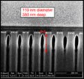
Fabrication of photonic crystals in GaN is complicated by the difficulty of etching the material, which is extremely hard and chemically inert. The structures are therefore fabricated by dry-etching using a chlorine-based plasma. Submicron patterning is performed using electron-beam, interferometric, or nano-imprint lithography. Figure 2 shows a focused-ion-beam scanning-electron-microscope image of a photonic lattice etched into GaN. The pattern shown here is a triangular lattice with a pitch of 205nm, a hole diameter of 110nm, and a hole depth of 380nm. The straight sidewalls and high (depth to width) aspect ratio of greater than 3:1 are desirable features for efficient light extraction.
Figure 2. A regular array of deep narrow holes etched into GaN forms a photonic crystal with a lattice constant of 205nm.
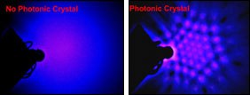
Research done partly at Sandia combined LED and photonic-crystal processing to make an electrically-injected InGaN LED. 3 Figure 3 shows the far-field-emission patterns for both a photonic-crystal and a control LED. The photonic-crystal LEDs strongly-modified far-field pattern shows a triangular symmetry due to the extraction of waveguided modes and showed a 50% increase in efficiency compared to the controls.
Figure 3. Far-field emission patterns from a conventional (left) and a photonic-crystal LED (right) are very different. The latter has a strongly-modified emission pattern due to the scattering of waveguided modes out of the LED chip.
Many InGaN LED performance improvements are still required, including increased efficiencies, higher power lamps, and lower cost per lamp. Photonic crystals have the potential to dramatically increase InGaN LED efficiency, a first step towards producing white-light at of 200lm/W.
{mosgoogle}
The authors would like to acknowledge the contributions made at Sandia National Laboratories by J. R. Wendt, R. J. Shul, S. H. Kravitz, K.W. Fullmer, and C. F. Schmidt; at Lumileds Lighting by J. J. Wierer and M. R Krames; and at the University of New Mexico by D. Li and S. R. J. Brueck. This work was supported by the Department of Energy's Office of Energy Efficiency and Renewable Energy (EERE). Sandia is a multiprogram laboratory operated by Sandia Corporation, a Lockheed Martin Company, for the United States Department of Energy's National Nuclear Security Administration under contract DE-AC04-94AL85000.
Authors
Daniel L. Barton and Arthur J. Fischer
Semiconductor Material and Device Sciences, Sandia National Labs. Albuquerque, NM Dr. Barton has authored and presented several contributed and invited papers at SPIE Photonics West including a chapter in an SPIE critical review book on gallium nitride-based technologies.http://www.sandia.gov/1100 Dr. Fischer is a Principal Memeber of the Technical Staff at Sandia National Laboratories. He has been leading the research at Sandia on photonic crystals for solid state lighting and other potential applications.
References:
1. S. J. Smith, E. M. Purcell, Visible Light from Localized Charges Moving across a Grating, Phys. Rev, Vol: 92, no. 4, pp. 1069, 1953.
2. E. Yablanovich, Inhibited Spontaneous Emission in Solid-State Physics and Electronics, Phys. Rev. Lett., Vol: 55, no. 20, pp. 2059, 1987.
3. Jonathan J. Wierer, Michael R. Krames, John E. Epler, Nathan F. Gardner, Joel R. Wendt, Mihail M. Sigalas, Steven R. J. Brueck, Dong Li, Michael Shagam, III-nitride LEDs with photonic crystal structures, Proc. SPIE, Vol: 5739, pp. 102-107, 2005.


