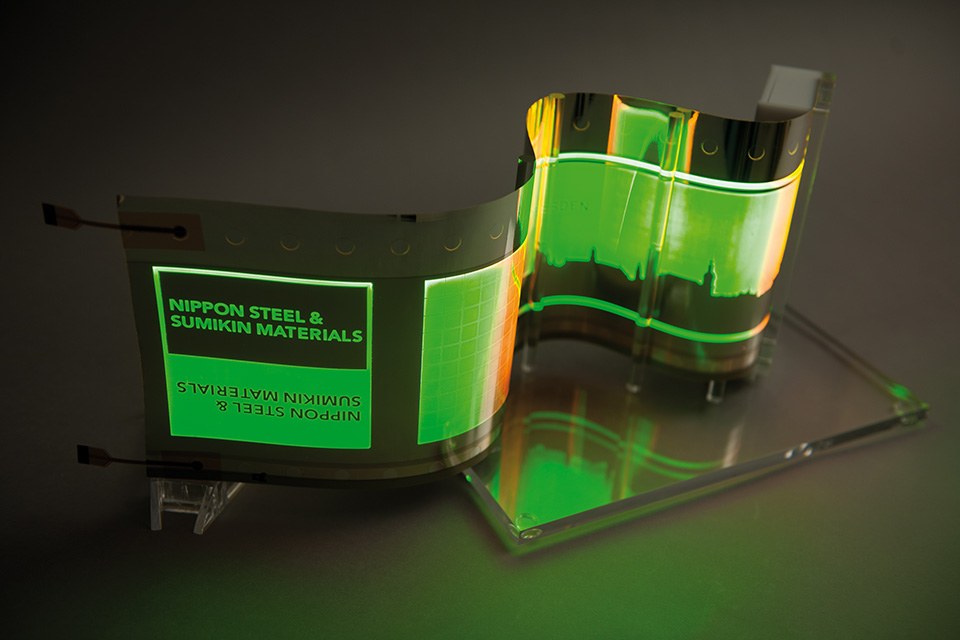
OLEDs Applied to Paper-Thin Stainless Steel
Fraunhofer Institute for Organic Electronics, Electron Beam and Plasma Technology FEP, a provider of R&D in the field of organic electronics, will be presenting OLEDs on gauzy stainless steel foil during aimcal 2017 in Tampa/USA, from October 15-18, 2017. The novel application on display in Booth 22 was developed in cooperation with the Nippon Steel & Sumikin Materials Co., Ltd. (NSMAT) and Nippon Steel & Sumitomo Metal Corporation (NSSMC).
Stainless steel is normally associated with kitchenware and chemical Plant pipe. However, stainless steel foil has also been utilized for several years in thin-film photovoltaics and batteries. Now stainless steel can also serve as a substrate for flexible electronic components. In comparison to the conventional substrate materials like glass or plastic web the material possesses special properties for this purpose and is well-suited as a substrate for organic light-emitting diodes (OLEDs), for example. Thanks to the planarization layer developed by NSSMC as well as the comparatively good thermal conductivity of stainless steel, homogenous large-area lighting surfaces with current densities of more than 10 mA/cm² have become better applicable.
Moreover, OLEDs need to be protected from water vapor and oxygen in order that the organic layers remain fully functional. Stainless steel provides excellent barrier properties against environmental influences and is therefore suitable as a substrate for OLEDs from this standpoint as well.
Jun Nakatsuka, Manager of Business Development at NSMAT, is looking to the future: “Thanks to the smoothness and high thermal conductivity of the stainless steel foil we obtain extremely homogenous OLED light. We see OLEDs on stainless steel in perhaps three years from now being used in automobiles as turn indicator and back-up lights, as cladding for fascia, and as advertising displays.”
There is some ways to go before reaching that juncture. Following the expensive development of stainless steel foil, it still needs to be made suitable for production purposes. Fraunhofer FEP has at its disposal roll-to-roll processing lines for manufacturing OLEDs on flexible materials and an OLED process that has high reproducibility. This is what has made possible the development of stainless steel foil with a clean and smooth planarization layer.
Michael Stanel, Project Manager within the R2R Organic Technology department at Fraunhofer FEP explains: “In addition to machinery design and construction, we also possess comprehensive know-how in handling sensitive substrates. To be certain the stainless steel is suitable for the nanometer-thick organic layers, an R2R-compatible smoothing planarization layer was developed that is easy to integrate into the process.”
It was also important during the collaboration with NSMAT and NSSMC to work out quality standards for the future OLED fabrication. In particular, the surface properties of the substrate were specified and are being continuously improved in cooperation with NSMAT and NSSMC.
Fraunhofer FEP at aimcal 2017: Trade Fair booth: No. 22
About Fraunhofer FEP:
The Fraunhofer Institute for Organic Electronics, Electron Beam and Plasma Technology FEP is located in Dresden and focuses on developing innovative solutions, technologies and processes for surface modification and organic electronics.
Our core technologies are electron beam technology, sputtering technology, plasma-activated high-rate deposition, high-rate PECVD, and technologies for organic electronics and IC-/System design, which we use to develop solutions for various industrial tasks in surface treatment, vacuum coating and for organic semiconductors.
We offer a broad range of research, development and pilot manufacturing opportunities, especially for the treatment, structuring and finishing of surfaces as well as for OLED microdisplays, organic and inorganic sensors, optical filters and flexible OLED lighting. Our fields of work are subdivided into 7 business units based on the different materials and geometries being processed and due to special technological synergies.
The deposition of single layers and multilayer systems as well as the processing of surfaces are of huge practical importance across all industries. In addition, the development and integration of flexible organic electronics, OLED devices and OLED-on-silicon technologies offers a wide range of advantages and possibilities for novel applications such as wearables, data glasses, flexible lighting or microdisplays with sensor functions in environmental or medical solutions.
Whether in mechanical engineering, for use of solar energy in the field of smart building and architecture, in packaging industry, biomedical engineering, agriculture, preservation or in optics, sensor technology and electronics sector: We develop suitable processes and technologies as well as appropriate prototypes, devices and technological key components for our industrial customers as well as partners from research, scientific or public sectors from all over the world.
Feasibility studies, to evaluate surface coating or the integration of organic electronics in devices and pilot production, to facilitate the introduction of new customer products to the market, are also included in our range of services. The upscaling of technologies to industrial quantities and the integration into suitable plant technology and into existing production processes as well as the possibility of technology transfer and licensing are essential services of our institute. The cost efficiency of a technology for industrial production is always taken into account.
Together with companies, research institutions and public institutions we are working on novel, pioneering technologies within public funded projects of various funding authorities. By this we are continuously enhancing our comprehensive know how, which sets the basis to support our customers with their research and development projects from the first concept phase up to industrial realization.

