Novel Nano-Etched Cavity Makes LEDs 7 Times Brighter
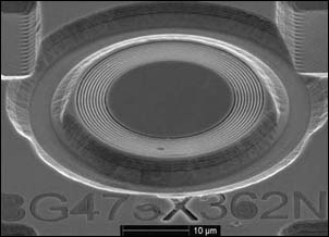
Researchers at the National Institute of Standards and Technology (NIST) have made semiconductor light-emitting diodes (LEDs) more than seven times brighter by etching nanoscale grooves in a surrounding cavity to guide scattered light in one direction.
The novel nanostructure, which may have applications in areas such as in biomedical imaging where LED brightness is crucial, is described in the July 17 issue of Applied Physics Letters.*
Semiconductor LEDs are used increasingly in displays and many other applications, in part because they can efficiently produce light across a broad spectrum, from near-infrared to the ultraviolet. However, they typically emit only about two percent of the light in the desired direction: perpendicular to the diode surface. Far more light skims uselessly below the surface of the LED, because of the extreme mismatch in refraction between air and the semiconductor. The NIST nanostructured cavity boosts useful LED emission to about 41 percent and may be cheaper and more effective for some applications than conventional post-processing LED shaping and packaging methods that attempt to redirect light.
The NIST team fabricated their own infrared LEDs consisting of gallium arsenide packed with "quantum dots" of assorted sizes made of indium gallium arsenide. Quantum dots are nanoscale semiconductor particles that efficiently emit light at a color determined by the exact size of the particle. The LEDs were backed with an alumina mirror to reflect the light emitted backwards. The periphery of each LED was turned into a cavity etched with circular grooves, in which the light reflects and interferes with itself in an optimal geometry.
The researchers experimented with different numbers and dimensions of grooves. The brightest output was attained with 10 grooves, each about 240 nanometers (nm) wide and 150 nm deep, and spaced 40 nm apart. The team spent several years developing the design principles and perfecting the manufacturing technique. The principles of the method are transferable to other LED materials and emission wavelengths, as well as other processing techniques, such as commercial photolithography, according to lead author Mark Su.
* M.Y. Su and R.P. Mirin. Enhanced light extraction from circular Bragg grating coupled microcavities. Applied Physics Letters. July 17.


