In New Quantum-Dot LED Design, Researchers Turn Troublesome Molecules to Their Advantage
By nestling quantum dots in an insulating egg-crate structure, researchers at the Harvard School of Engineering and Applied Sciences (SEAS) have demonstrated a robust new architecture for quantum-dot light-emitting devices (QD-LEDs).
Quantum dots are very tiny crystals that glow with bright, rich colors when stimulated by an electric current. QD-LEDs are expected to find applications in television and computer screens, general light sources, and lasers.
Previous work in the field had been complicated by organic molecules called ligands that dangle from the surface of the quantum dots. The ligands play an essential role in quantum dot formation, but they can cause functional problems later on.
Thanks to an inventive change in technique devised by the Harvard team, the once-troublesome ligands can now be used to build a more versatile QD-LED structure. The new single-layer design, described in the journal Advanced Materials, can withstand the use of chemical treatments to optimize the device's performance for diverse applications.
"With quantum dots, the chemical environment that's optimal for growth is usually not the environment that's optimal for function," says co-principal investigator Venkatesh Narayanamurti, Benjamin Peirce Professor of Technology and Public Policy at SEAS.
The quantum dots, each only 6 nanometers in diameter, are grown in a solution that glows strikingly under a black light.
The solution of quantum dots can be deposited onto the surface of the electrodes using a range of techniques, but according to lead author Edward Likovich (A.B. ’06, S.M. ’08, Ph.D. ’11), who conducted the research as a doctoral candidate in applied physics at SEAS, "That's when it gets complicated."
"The core of the dots is a perfect lattice of semiconductor material, but on the exterior it's a lot messier," he says. "The dots are coated with ligands, long organic chains that are necessary for precise synthesis of the dots in solution. But once you deposit the quantum dots onto the electrode surface, these same ligands make many of the typical device processing steps very difficult."
The ligands can interfere with current conduction, and attempts to modify them can cause the quantum dots to fuse together, destroying the properties that make them useful. Organic molecules can also degrade over time when exposed to UV rays.
Researchers would like to be able to use those ligands to produce the quantum dots in solution, while minimizing the negative impact of the ligands on current conduction.
“The QD technologies that have been developed so far are these big, thick, multilayer devices,” says co-author Rafael Jaramillo, a Ziff Environmental Fellow at the Harvard University Center for the Environment. Jaramillo works in the lab of Shriram Ramanathan, Associate Professor of Materials Science at SEAS.
“Until now, those multiple layers have been essential for producing enough light, but they don't allow much control over current conduction or flexibility in terms of chemical treatments. A thin, monolayer film of quantum dots is of tremendous interest in this field, because it enables so many new applications.”
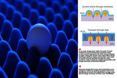
The new QD-LED resembles a sandwich, with a single active layer of quantum dots nestled in insulation and trapped between two ceramic electrodes. To create light, current must be funneled through the quantum dots, but the dots also have to be kept apart from one another in order to function.
In an early design, the path of least resistance was between the quantum dots, so the electric current bypassed the dots and produced no light.
Abandoning the traditional evaporation technique they had been using to apply insulation to the device, the researchers instead used atomic layer deposition (ALD)—a technique that involves jets of water. ALD takes advantage of the water-resistant ligands on the quantum dots, so when the aluminum oxide insulation is applied to the surface, it selectively fills the gaps between the dots, producing a flat surface on the top.
"Exploiting these hydrophobic ligands allowed us to insulate the interstices between the quantum dots, essentially creating a structure that acts as an egg crate for quantum dots," says co-author Kasey Russell (A.B. '02, Ph.D. '09), a postdoctoral fellow at SEAS. "The benefit is that we can funnel current directly through the quantum dots despite having only a single layer of them, and because we have that single layer, we can apply new chemical treatments to it, moving forward."
Through Harvard's Office of Technology Development, Likovich and his colleagues have applied for a provisional patent on the device. Beyond the possible applications in computer and TV displays, lights, and lasers, the technology could one day be used in field-effect transistors or solar cells.
The research was supported by the Harvard University Center for the Environment; the Nanoscale Science and Engineering Center at Harvard, which is funded by the National Science Foundation (NSF); and the use of facilities at the Harvard University Center for Nanoscale Systems, a member of the NSF-supported National Nanotechnology Infrastructure Network.


