Intellectual Properties
IP, Reports & Roadmaps
|
Aug 03, 2010
BridgeLux responds to Cree lawsuit
Sunnyvale, California, USA, BridgeLux, Inc., a leading supplier of energy saving LED chips to high-volume solid state lighting market segments, confirmed that on September 12, 2006, it was served in a lawsuit filed by Cree, Inc. and Boston University alleging infringement of US Patent Numbers 6,657,236 and 5,686,738.
Read more »
IP, Reports & Roadmaps
|
Aug 03, 2010
Competitive Technologies to commercialize optical technology for LED lighting market
Competitive Technologies, Inc. today announced that it has signed an exclusive, worldwide service and representation agreement with Illumitex, LLC to license optical technology for the light emitting diode ("LED") industry. The technology is a fundamental and enabling primary optical device that significantly improves the effectiveness of High Brightness LEDs ("HBLEDs").
Read more »
IP, Reports & Roadmaps
|
Aug 03, 2010
Cree files lawsuit against bridgeLux for patent infringement
DURHAM, NC, Cree, Inc. (Nasdaq: CREE), a leader in LED solid-state lighting components, today announced that it has filed suit against BridgeLux, Inc. (formerly eLite Optoelectronics) for infringement of U.S. Patent Nos. 6,657,236 (“the ‘236 patent”) and 5,686,738 (“the ‘738 patent”).
Read more »
IP, Reports & Roadmaps
|
Aug 03, 2010
External extraction light emitting diode based upon crystallographic faceted surfaces
 A light emitting diode is disclosed that includes a support structure and a Group III nitride light emitting active structure mesa on the support structure. The mesa has its sidewalls along an indexed crystal plane of the Group III nitride. A method of forming the diode is also disclosed that includes the steps of removing a substrate from a Group III nitride light emitting structure that includes a sub-mount structure on the Group III nitride light emitting structure opposite the substrate, and thereafter etching the surface of the Group III nitride from which the substrate has been removed with an anisotropic etch to develop crystal facets on the surface in which the facets are along an index plane of the Group III nitride. The method can also include etching the light emitting structure with an anisotropic etch to form a mesa with edges along an index plane of the Group III nitride.
Read more »
IP, Reports & Roadmaps
|
Aug 03, 2010
High efficiency light emitting diode (LED) with optimized photonic crystal extractor
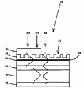 A high efficiency, and possibly highly directional, light emitting diode (LED) with an optimized photonic crystal extractor. The LED is comprised of a substrate, a buffer layer grown on the substrate (if needed), an active layer including emitting species, one or more optical confinement layers that tailor the structure of the guided modes in the LED, and one or more diffraction gratings, wherein the diffraction gratings are two-dimensional photonic crystal extractors. The substrate may be removed and metal layers may be deposited on the buffer layer, photonic crystal and active layer, wherein the metal layers may function as a mirror, an electrical contact, and/or an efficient diffraction grating.
Read more »
IP, Reports & Roadmaps
|
Aug 03, 2010
Epistar licenses unique LED technology from ITRI
Taipei, Epistar Corp., a leading Taiwanese supplier of light emitting diode (LED) chips, has recently licensed a unique technology for boosting LED lumen from the government-backed Industrial Technology Research Institute (ITRI), making its patent deployment more complete.
Read more »
IP, Reports & Roadmaps
|
Aug 03, 2010
Color Kinetics and Robe Show Lighting announce licensing agreement
 Boston, MA, USA and Hazovice, Czech Republic, Color Kinetics Incorporated (NASDAQ: CLRK) and Robe Show Lighting, respective market leaders in LED and entertainment lighting, today announced a global licensing agreement whereby Robe will have access to Color Kinetics' complete patent portfolio, enabling the development and sale of its LED Series and Anolis product lines.
Read more »
IP, Reports & Roadmaps
|
Aug 03, 2010
Ya Hsin acquires Osram’s LED technology for general lighting
Taipei, Ya Hsin Industrial Co., Ltd. will become the first Taiwanese manufacturer to license white-LED technology for general lighting purpose from Osram should the two companies sign an agreement early next month.
Read more »
IP, Reports & Roadmaps
|
Aug 03, 2010
Sidley Austin LLP announces client settlement of patent infringement claims against LED manufacturer
Sidley Austin LLP announced today that the firm represented Professor Gertrude Neumark Rothschild in her settlement of claims of patent infringement against Toyoda Gosei Co. Ltd., and Toyoda Gosei North America Corporation.
Read more »
IP, Reports & Roadmaps
|
Aug 03, 2010
TIR surpasses milestone of 100 patent filings: TIR'S Leadership in SSL technology creates demand for speaking engagements and technical papers
Vancouver, BC – TIR Systems Ltd. (TSX: TIR), announces that as of August 1, the company has 113 patent applications in addition to six patents already granted in the field of Solid State Lighting (SSL).
Read more »
IP, Reports & Roadmaps
|
Aug 03, 2010
LED driver
 A light emitting diode (LED) driver to drive an LED, including a current adjusting unit to adjust magnitude of a current flowing on the LED by supplying power from a power supply device to the LED and cutting off the power. A modulation control unit is provided to modulate a waveform of the current flowing on the LED by controlling the adjustment operation of the current adjusting unit. A constant current offset unit to control the adjustment operation of the current adjusting unit is provided so that the current flowing on the LED is higher or equal to a predetermined value as the waveform thereof is modulated. Thus, provided is an LED driver having improved power consumption efficiency.
Read more »
IP, Reports & Roadmaps
|
Aug 03, 2010
Side view led package having lead frame structure designed to improve resin flow
 The invention relates to a side view LED package in use with an LCD backlight unit. The side view LED package comprises: an LED chip; and a strip-shaped lead frame having a toothed structure formed in a lateral edge thereof. The LED chip is mounted on a surface of the lead frame. An integral package body is made of resin, and includes a hollow front half having a cavity for housing the LED chip and a solid rear half divided from the front half by the lead frame. The toothed structure of the lead frame structure can improve resin flow in order to ensure stability even if the LED package is made extremely thin.
Read more »
IP, Reports & Roadmaps
|
Aug 03, 2010
Method of making a vertical light emitting diode
 Methods are disclosed for forming a vertical semiconductor light emitting diode (VLED) device having an active layer between an n-doped layer and a p-doped layer; and securing a plurality of balls on a surface of the n-doped layer of the VLED device.
Read more »
IP, Reports & Roadmaps
|
Aug 03, 2010
Semiconductor light emitting diode having textured structure and method of manufacturing the same
IP, Reports & Roadmaps
|
Aug 03, 2010
High output light emitting diode and method for fabricating the same
 A high output light emitting diode (LED) and a method for fabricating the LED is disclosed. The LED includes a sidewall or surface that is inclined. A reflective film is formed on the inclined sidewall or surface to allow light to reflect from the reflective film and to emit the light upward or in a favorable direction with respect to the device, thereby being configured and enabled to improve a light output of the LED and dispense with an additional passivation process.
Read more »
IP, Reports & Roadmaps
|
Aug 03, 2010
LED lighting system
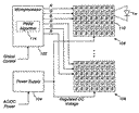 Method and system are disclosed for compensating for color variations due to thermal differences in LED based lighting systems. The method and system involves characterizing the LEDs to determine what PWM (pulse-width modulation) is needed at various operating temperatures to achieve a desired resultant color. The characterization data is then stored in the microprocessor either in the form of a correction factor or as actual data. When an operating temperature that is different from a calibration temperature is detected, the characterization data is used to adjust the PWM of the LEDs to restore the LEDs to the desired resultant color.
Read more »
IP, Reports & Roadmaps
|
Aug 03, 2010
Thin gallium nitride light emitting diode device
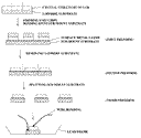 Disclosed is a light emitting diode (LED) device that comprises a crystal structure of a sapphire substrate-free gallium nitride (GaN) LED, wherein the crystal structure is mounted on a first surface of a sub-mount substrate in the form of a unit chip, and the first surface of the sub-mount substrate has a surface area greater than the surface area of a region in which the unit chip is bonded. Preforms for manufacturing the LED device and a method for manufacturing the LED device are also disclosed. The sapphire substrate, on which the crystal structure of the light emitting diode has grown, is processed into a unit chip before being removed. Thus, any crack in the crystal structure of the light emitting diode that may occur during the removal of the sapphire substrate can be prevented. Therefore, a thin light emitting diode device can be manufactured in a mass production system.
Read more »
IP, Reports & Roadmaps
|
Aug 03, 2010
Organic light emitting diode (oled) having improved stability, luminance, and efficiency
 An organic light emitting diode (OLED) includes a relatively thin diamnond-like carbon (DLC) layer disposed between the anode and the hole transport layer to improve luminous efficiency and operating life time. The relatively thin DLC layer inhibits hole injection, which balances charge flow and improves efficiency, and increases the surface smoothness of the anode, which contributes to the increased operating life time.
Read more »
IP, Reports & Roadmaps
|
Aug 03, 2010
Light emitting diode package having multiple molding resins
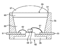 Disclosed is a light emitting diode (LED) package having multiple molding resins. The LED package includes a pair of lead terminals. At least portions of the pair of lead terminals are embedded in a package main body. The package main body has an opening through which the pair of lead terminals is exposed. An LED die is mounted in the opening and electrically connected to the pair of lead terminals. A first molding resin covers the LED die. A second molding resin with higher hardness than the first molding resin covers the first molding resin. Therefore, stress to be imposed on the LED die can be reduced and the deformation of the molding resins can be prevented.
Read more »
IP, Reports & Roadmaps
|
Aug 03, 2010
Programmable driving method for light emitting diode
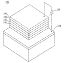 A programmable driving method for light emitting diode is disclosed, which is capable of providing a programmable multi-phase segment and a corresponding programmable multi-phase actuating signal to an LED with respect to user specification, such that an optimal driving sequence can be provided to the LED according to the requirements of the manufacturing process of a LED display and thus enabling the performance of the gray levels displayed by the LED display to be optimized.
Read more »
