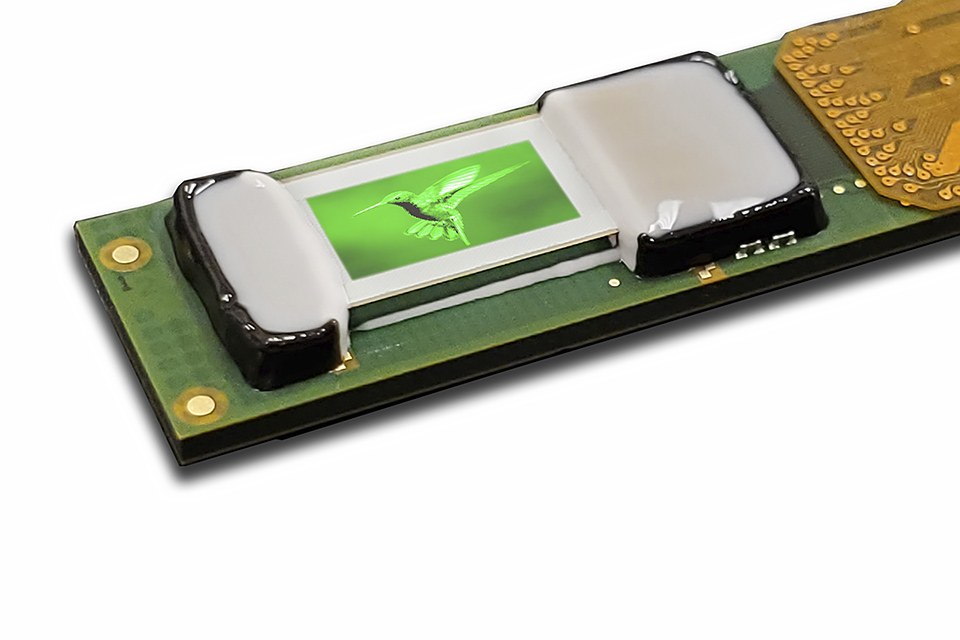
Compound Photonics and Plessey Create microLED Display Modules from Bonded Wafers
Compound Photonics US Corporation (CP), a leading provider of compact high-resolution microdisplay solutions for Augmented Reality (AR) and Mixed Reality (MR) applications, and Plessey Semiconductors Ltd. (Plessey), an embedded technologies developer at the forefront of microLED technology for AR and MR display applications, today announced they have produced the first fully addressable microLED display modules resulting from their previously announced strategic partnership to develop and introduce GaN-on-Silicon microLED based microdisplay solutions for AR/MR applications.
CP and Plessey engineering teams have successfully fabricated functional microLED display modules combining CP's industry-leading high speed digital low-latency display backplane with Plessey's breakthrough GaN-on-Silicon monolithic microLED array technology. Plessey's team produced the microLED array wafer bonded to CP's backplane wafer at its Plymouth, UK, facility. In turn, CP's team assembled and packaged display modules from the bonded wafer pair at its Phoenix, AZ, USA, facility. Both teams are currently performing initial characterization work at CP's Vancouver, WA, USA, facility.
"Today's milestone achievement is a direct result of the close working relationship between Plessey and CP development teams," commented Mike Lee, President of Corporate and Business Development at Plessey. "This successful proof-of-concept demonstration validates both companies' goals to produce the industry's highest performance microLED display modules that deliver improved brightness at the smallest pixel sizes, higher frame rates, with extended bit depth at the lowest power consumption to best serve next-generation emissive display-based AR/MR smart glasses and Heads-Up/Head-mounted displays (HUD/HMDs) applications."
Yiwan Wong, Compound Photonics' CEO, added: "These prototype microLED displays provide important confirmation that Plessey's monolithic GaN-on-Silicon IP, fabrication technology and bonding processes match perfectly with CP's industry leading 3.015 micron pixel pitch 1080p (1920x1080 pixel) backplane design to deliver compact high resolution microdisplays. Combined with CP's NOVA high-performance display driver architecture, these microLED displays support an industry standard MIPI interface to take advantage of CP's unique display pipeline solution designed for the real time needs of AR/MR applications. CP's display drive technology is extensible across multiple display technologies enabled by full software configurability, allowing customers to build their systems for specific power and performance needs."
Initial samples of a 0.26 inch diagonal, Full HD 1080p resolution microLED display module integrated with display driver IC and MIPI input are expected to be available by summer of 2020.
About Compound Photonics:
Compound Photonics is a pioneer in compact high resolution microdisplay technologies. CP's microdisplay solutions are optimized to serve the augmented reality and mixed reality markets where high performance, small form factor, and low power consumption are most critical. Compound Photonics' microdisplays enable engineers to innovate and create cutting edge consumer and industrial products that can greatly enhance the lives of people. CP offers customers an easy migration path for AR/MR display solutions from CP's existing production ready amplitude LCoS (Liquid Crystal on Silicon) reflective displays for immediate-term needs, to emerging microLED displays for mid-term needs, and ultimately to a true holographic 3D display solution via CP's phase LCoS display solution in the future. - www.compoundphotonics.com
About Plessey:
Plessey is an award-winning provider of full-field emissive microLED displays that combine very high-density RGB pixel arrays with high-performance CMOS backplanes to produce very high-brightness, low-power and high-frame-rate image sources for head-mounted displays (HMDs), and augmented reality (AR) and virtual reality (VR) systems. Plessey operates leading-edge 150mm and 200mm wafer processing facilities to undertake design, test and assembly of LED products, and a comprehensive suite of photonic characterization and applications laboratories. For more information, visit Plessey's website at plesseysemiconductors.com

