USHIO America - World's First 6-Inch Full-Field Projection Exposure System for Manufacturing LED Chips
USHIO America, a leading provider of specialty and general illumination lighting solutions as a wholly owned subsidiary of USHIO Inc, today announced that the company has started marketing the world’s first 6-inch full-field projection exposure system for manufacturing LED chips in the US.
For manufacturing light-emitting diodes (LEDs), exposure equipment has been used to form electrodes, electrical circuitry, and a passivation layer on a sapphire wafer used as the substrate, in the same manner as for manufacturing semiconductor devices. In general, stepper systems (step & repeat projection exposure systems) or contact exposure systems used for manufacturing semiconductors have been also used for 2-inch or 4-inch sapphire wafers.
As applications of LEDs have increased, the demand has increased dramatically while the price has been lowered significantly. In order to meet the growing need, LED chip manufacturers have increased wafer sizes from 2-inch or 4-inch wafers to 6-inch wafers in order to enhance productivity and reduce manufacturing cost by increasing the number of chips produced from each wafer.
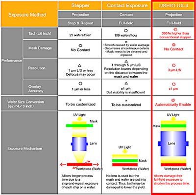
The increase in wafer size, however, has caused such problems as a warpage or distortion of wafers that cannot be eliminated by conventional stepper or contact exposure systems, thus lowering the yield due to deposition errors. In addition, these conventional exposure systems require changes in system settings and replacement of parts for wafer size conversion. This can cause additional cost and downtime, so that it has been a challenge in technology and cost to enhance productivity by increasing wafer size.
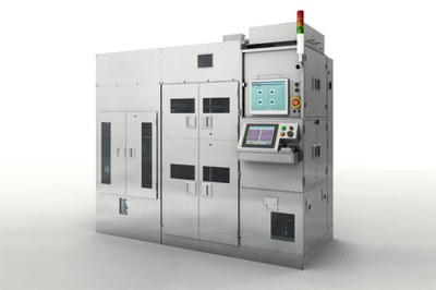
USHIO successfully developed its new exposure system — model UX4-LEDs —that allows full-field exposure of 6-inch wafers while preventing wafer warpage or distortion, achieving a throughput enhancement of 300% compared with conventional stepper systems. The UX4-LEDs exposure system is based on the same platform as USHIO’s field-proven UX series full-field projection exposure systems for semiconductors, FPDs, printed-circuit boards and MEMS. USHIO already has installed more than 1,000 units of the UX series systems throughout the world.
“The UX4-LEDs projection exposure system is one of the most innovative items of LED manufacturing equipment today. Based on a collection of our lighting-edge technologies that USHIO has fostered in its field-proven UX exposure system series, it is the world’s first 6-inch wafer full-field projection exposure system. It will allow major LED manufacturers to dramatically increase their mass-production capacity while lowering their manufacturing cost,” said Kenji Hamashima, President/CEO of USHIO America. “We are confident of introducing this new product into the US market and gaining top market share by reinforcing our sales and technical support forces. We expect to ship the first unit within this year, since several major LED manufactures have already been evaluating this system for mass-production.”
Full-field Projection Exposure Up to 6-inch Wafers:
• Requires no contact between the mask and wafer, thus avoiding potential damage to both and preventing any defect on a circuit pattern.
• Requires neither mask replacement nor cleaning that would cause system downtime.
• Allows full-field exposure to enhance throughput (300% higher than that of conventional stepper systems)
High Overlay Accuracy and High Resolution:
• USHIO originally developed the projection lens and the alignment and wafer transfer mechanism optimized for manufacturing LEDs.
• Allows enhancement of detection accuracy of alignment marks with low visibility, such as those for transparent electrodes, to achieve high overlay accuracy.
• Original wafer chucking method for eliminating warpage or distortion of wafers, and a projection lens with a deep depth of focus minimize variation in line width.
Flexible System Design:
• Designed to automatically handle wafer size conversions so as to allow an increase in wafer size without changing system settings or replacing parts, thus requiring no downtime.
• Use of modular structure for major system components allows easy specification changes or upgrading as well as easy maintenance.
High Cost-Benefit Performance:
• Designed specifically for LED manufacturing to greatly reduce the initial cost compared with use of a semiconductor stepper system for manufacturing LEDs.
• Running cost is reduced by 80% of the conventional stepper systems to lower the cost of ownership (CoO).
• The footprint reduced by 50% or more from the conventional UX series to achieve 3.0 m2 or less.


