Translucent Announces Commercial Availability of vGaN™ Wafer Templates for Low-Cost Epitaxial Growth of GaN Devices
Translucent, Inc., a provider of rare-earth-oxide (REO) engineered silicon substrates for low-cost, high-performance epitaxial semiconductorapplications, announced today the commercial availability of its vGaN™ family of silicon-based wafer templates. The vGaN products provide a low-cost, high-quality epitaxial surface for the growth of gallium nitride (GaN) devices such as light-emitting diodes (LEDs) or field-effect transistors (FETs).
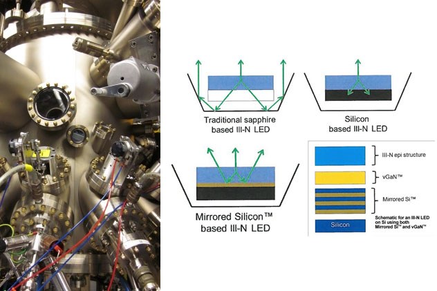
The vGaN product line is the world’s first commercial REO-based family of ‘III-N semiconductors’ with scalable GaN-on-Si wafers. Translucent’s use of crystalline REO layers provides stress relief and wafer flatness through customized lattice engineering, leading to a high quality growth surface. In addition, the wide bandgap of the REO layer is expected to lead to much higher breakdown-voltage characteristics for FETs grown on vGaN.
vGaN stands for “virtual gallium nitride.” It provides a semiconductor growth surface that has the physical properties of GaN, but utilises a silicon substrate upon which is grown an epilayer of REO material that accommodates a top epilayer of Group III nitrides such as GaN. The vGaN substrate enables for the first time, industry-standard MOCVD growth processes with the low cost structures and economies of scale currently enjoyed by the silicon industry.
Michael Lebby, Translucent’s general manager, noted, “We are bringing a decade of Translucent REO epitaxial experience to bear on the challenge of enabling GaN growth to scale cost-effectively well beyond current limitations. Our vGaN platform is an ‘on-silicon’ technology, allowing us to harness mature silicon-substrate technologies and their low costs, and we expect this to have an extremely beneficial impact in driving down costs for GaN-based LEDs and FETs.”
GaN is typically grown on sapphire substrates, which are significantly more expensive at large diameters, especially 200 mm and larger. Additionally, a major challenge facing device manufacturers today is the handling of the large, heavy, and expensive sapphire wafers. Such handling may require the purchase of special handling equipment for the fabrication plants. Conversely, the widely-used infrastructure of fabrication plants that are ready to run silicon wafers up to 200 mm already exists. This makes large-diameter silicon an ideal choice to bring economies of scale into the lighting (LED) and power electronics (FET) industries.
Translucent’s vGaN wafers are already available today at 100 mm diameters, with 150 and 200 mm becoming available during the next year.
About Translucent:
Translucent, Inc., a subsidiary of Australian listed company Silex Systems Limited. (SLX: ASX), is an advanced materials company founded in 2001 that focuses on using rare-earth oxides to provide low-cost, silicon-based templates for epitaxial growth of semiconductors. With its emphasis on GaN- and GaAs-compatible growth platforms, Translucent is developing products for the solar, power FET, and solid-state lighting (LED) industries. vGaN is a registered trademark of Translucent, Inc. More information is available at www.translucentinc.com and www.silex.com.au.


