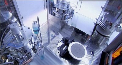
EV Group Introduces Industry's First Fully Automated Wafer Bonding System for High-Brightness LED Manufacturing
EV Group (EVG), a leading supplier of wafer bonding and lithography equipment for the MEMS, nanotechnology and semiconductor markets, today announced that it has introduced the EVG560HBL wafer bonder-the industry's first fully automated wafer bonding system for high-brightness light emitting diode (HB-LED) manufacturing.
The system features a new design for multi-substrate bonding and is capable of throughput rates of an unprecedented 160 bonds per hour. Based on the successful EVG500 wafer bonding series, the EVG560HBL is optimized to meet the unique requirements of HB-LED manufacturers with the advanced automation capabilities that they will need to increase their production capacity and yields.
The HB-LED market continues to grow at a rapid pace due to the rising number of applications that can take advantage of the lower energy consumption and myriad other benefits of LED devices. According to market research firm Strategies Unlimited (Mountain View, Calif.), the HB-LED market will grow from $8.2 billion in 2010 to $20.2 billion by 2014, driven mainly by the market for LCD display backlights and lighting applications. To meet this increased demand, HB-LED manufacturers must quickly ramp up to higher production capacity, as well as optimize their manufacturing processes to ensure the highest yields-both of which drive the need for automated manufacturing solutions. This is especially critical for the wafer bonding process, which is needed to transfer the active LED layer from epitaxial substrates onto carrier wafers with thermal properties better suited for HB-LED devices. With a dominant position in the wafer bonder market and having served the HB-LED industry for many years, EVG is uniquely positioned to leverage its expertise to bring the first dedicated automated wafer bonding solution to this industry.
"Through continuous investment and innovation in equipment manufacturing and process engineering expertise, EVG is bringing start-of-the-art processing solutions for high-volume manufacturing applications to our customers," stated Paul Lindner, executive technology director, EV Group. "Leveraging our 30 years of experience in developing wafer bonding solutions for advanced micro-electronics manufacturing, the EVG560HBL is the latest result in our ongoing efforts aimed at helping HB-LED manufacturers develop more efficient, cost-effective and higher yielding devices to meet the demands of their customers."
EVG560HBL System Features:
The EVG560HBL is a multi-substrate wafer bonder that offers a number of advanced capabilities to enable high-volume HB-LED manufacturing, including:
• High-force capability, in-situ low-force wedge compensation and proprietary compliant layer technologies-all to ensure bond uniformity across the entire wafer, which is essential for high-quality, multi-substrate bonding
• Integrated pre-processing modules for low-temperature metal wafer bonding, which enables higher throughput and provides less thermal stress on the wafer stack, which in turn increases yield
• Warped/bowed wafer handling capability for maneuvering thin and fragile substrates, which minimizes tool downtime and eliminates wafer breakage issues
• Unique bond chamber design, which enables customers to change out substrate sizes in less than 30 minutes, increasing tool flexibility and lifetime while enabling easy maintenance and maximized tool uptime
• Cassette-to-cassette operation
• Mechanical wafer-to-wafer alignment
• SECS II/GEM interface
• Wafer ID tracking for advanced process control
The EVG560HBL is available for purchase immediately. For more information about the EVG560HBL, please visit www.evgroup.com or download the EVG560HBL product fact sheet. You can also learn more about the new system and EVG's other HB-LED manufacturing solutions at SEMICON West (July 13-15) in San Francisco, Calif., where Dr. Thomas Uhrmann, Business Develop Manager, will be presenting "Wafer-level Packaging for Cost Reduction of High-brightness LEDs" on Wednesday, July 14 at 3:00 p.m. during the Extreme Electronics' Solid-state Lighting session, "More Lumens per Dollar: The Road to More Efficient HB-LED Manufacturing-Progress and Next Challenges in Back-end Manufacturing."
About EV Group:
EV Group (EVG) is a world leader in wafer-processing solutions for semiconductor, MEMS and nanotechnology applications. Through close collaboration with its global customers, the company implements its flexible manufacturing model to develop reliable, high-quality, low-cost-of-ownership systems that are easily integrated into customers' fab lines. Key products include wafer bonding, lithography/nanoimprint lithography (NIL) and metrology equipment, as well as photoresist coaters, cleaners and inspection systems.
In addition to its dominant share of the market for wafer bonders, EVG holds a leading position in NIL and lithography for advanced packaging and MEMS. Along these lines, the company co-founded the EMC-3D consortium in 2006 to create and help drive implementation of a cost-effective through-silicon via (TSV) process for major ICs and MEMS/sensors. Other target semiconductor-related markets include silicon-on-insulator (SOI), compound semiconductor and silicon-based power-device solutions.
Founded in 1980, EVG is headquartered in St. Florian, Austria, and operates via a global customer support network, with subsidiaries in Tempe, Ariz.; Albany, N.Y.; Yokohama and Fukuoka, Japan; Seoul, Korea and Chung-Li, Taiwan. The company's unique Triple i-approach (invent - innovate - implement) is supported by a vertical integration, allowing EVG to respond quickly to new technology developments, apply the technology to manufacturing challenges and expedite device manufacturing in high volume. More information is available at www.EVGroup.com.


