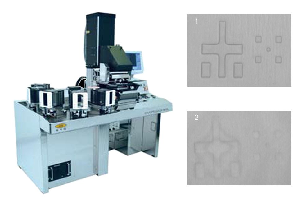
EV Group Expands Portfolio of Products to Address Fast-Growing HB-LED Market With Launch of EVG620HBL Mask Alignment System
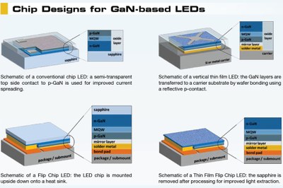
EV Group (EVG), a leading supplier of wafer-bonding and lithography equipment for the advanced semiconductor and packaging, MEMS, silicon-on-insulator (SOI) and emerging nanotechnology markets, announced the latest addition to its portfolio of products created to optimize the manufacture of high-brightness light-emitting diodes (HB-LEDs), compound semiconductors and power electronics. The new EVG620HBL fully automated mask alignment system builds on EVG's field-proven mask aligner platform, adding a high-intensity ultraviolet (UV) light source and five cassette stations – significantly more than competitive offerings – to enable continuous fabrication of devices. As a result, the EVG620HBL delivers unparalleled throughput of up to 165 six-inch wafers per hour (up to 220 wafers per hour in first print mode) with the industry's highest alignment accuracy and yield.
According to market research firm Global Information, Inc. (Farmington, Conn.), global consumption of high brightness LEDs (HB-LEDs) will continue to grow at a rapid pace over the next decade, from $10.09 billion in 2010 to $46.05 billion in 2020. Key drivers will include explosive growth in solid-state and general lighting applications, as well as signage, professional displays, and stationary (non-vehicle) signals. To meet this increased demand, HB-LED manufacturers must quickly ramp up to higher production capacity, as well as optimize their manufacturing processes to ensure the highest yields – all of which elevates their need for automated manufacturing solutions with the lowest cost of ownership.
As with its dedicated EVG560HBL automated wafer-bonding system, introduced last July, EVG developed the EVG620HBL aligner to address these needs. EVG is not new to this market – its bonders and mask aligners are being deployed by four of the top five major HB-LED manufacturers. Building on this success, the company created the 620HBL in response to customer demand for a mask alignment system dedicated to meeting these devices' yield and throughput requirements.
Another key feature of the EVG620HBL is the availability of special recipe-controlled microscopes whose illumination spectrum is optimized to ensure the best pattern contrast with various wafer and layer materials, including such advanced substrate materials as sapphire, silicon carbide (SiC), aluminum nitride (AlN), metal and ceramic.
"Our ongoing R&D efforts and focus on innovation in equipment manufacturing and process engineering are enabling EVG to consistently deliver the state-of-the-art, high-volume manufacturing solutions that our customers expect," stated Paul Lindner, EV Group's executive technology director. "Just last month, one of the leading HB-LED manufacturers ordered an EVG560HBL bonder, and the EVG620HBL is the latest result of our ongoing efforts around enabling HB-LED manufacturers to develop more efficient, cost-effective and higher yielding devices to meet their customers' demands. We look forward to making further inroads with this latest offering, which also features high-accuracy handling and alignment of fragile or warped wafers."
The EVG620HBL is available for purchase immediately. For more information, please visit www.evgroup.com/ or download the EVG620HBL product fact sheet. For media interested in learning more about the new system and EVG's other HB-LED manufacturing solutions, please contact Brandy Lee at blee@mcapr.com or +1-650-968-8900, ext.129.
About EV Group:
EV Group (EVG) is a world leader in wafer-processing solutions for semiconductor, MEMS and nanotechnology applications. Through close collaboration with its global customers, the company implements its flexible manufacturing model to develop reliable, high-quality, low-cost-of-ownership systems that are easily integrated into customers' fab lines. Key products include wafer bonding, lithography/nanoimprint lithography (NIL) and metrology equipment, as well as photoresist coaters, cleaners and inspection systems.
In addition to its dominant share of the market for wafer bonders, EVG holds a leading position in NIL and lithography for advanced packaging and MEMS. Along these lines, the company co-founded the EMC-3D consortium in 2006 to create and help drive implementation of a cost-effective through-silicon via (TSV) process for major ICs and MEMS/sensors. Other target semiconductor-related markets include silicon-on-insulator (SOI), compound semiconductor and silicon-based power-device solutions.
Founded in 1980, EVG is headquartered in St. Florian, Austria, and operates via a global customer support network, with subsidiaries in Tempe, Ariz.; Albany, N.Y.; Yokohama and Fukuoka, Japan; Seoul, Korea and Chung-Li, Taiwan. The company's unique Triple i-approach (invent - innovate - implement) is supported by a vertical integration, allowing EVG to respond quickly to new technology developments, apply the technology to manufacturing challenges and expedite device manufacturing in high volume. More information is available at www.evgroup.com/.


