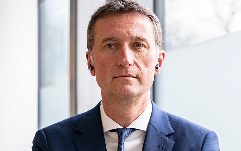
MicroLED Pioneer Aledia Has Appointed Pierre Laboisse as CEO
Laboisse, formerly the executive vice president at AMS-Osram, has stepped into the role previously held by Giorgio Anania. While Anania has transitioned to the company’s board of directors, Laboisse takes the helm.
Originating from the French research institute CEA-Leti in 2011, Aledia SA, based in Grenoble, France, set its sights on pioneering 3D microLED technology. This technology, rooted in gallium nitride nanowires, is crafted on expansive silicon wafers. As of now, Aledia employs 200 mm silicon wafers, but there's a vision to transition to 300 mm wafers to meet the demands of high-volume production.
In a significant move in 2019, Aledia laid the foundation for a 4,000 square meter pilot fab in Echirolles, close to Grenoble. This facility, dedicated to producing nanowire LEDs on 200mm-diameter wafers, came with a €20 million price tag.
Fast forward to 2020, and Aledia pinpointed Champagnier, a locale near Grenoble, as the chosen ground for a sprawling €50 million wafer fab designed for mass production.
BPI, a state-backed public investment bank, commented on Aledia's journey, emphasizing the imminent challenge: transitioning from development to the actual production and sale of their inaugural products.
The financial backing for Aledia's ventures, amounting to €120 million, is courtesy of its long-standing shareholders. Notable names in this list include CEA Investissement, Supernova Invest, and the SPI and Ecotechnologies funds, both under the stewardship of Bpifrance.
© 2023 Luger Research e.U. – Institute for Innovation & Technology

